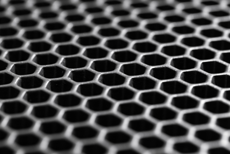
Northwestern University researchers have developed a novel method to host gas molecules as they are being analyzed in real time, using honeycomb structures found in nature as inspiration for an ultra-thin ceramic membrane they incorporated to encase the sample.
In addition to inferring the signatures of gas atoms through their unique bonds, the encapsulation strategy works within high-vacuum transmission electron microscopes (TEMs) to enhance imaging of solid nanostructures. These tools can be used across the board, from national labs conducting basic research to innovative start-ups creating practical applications.
When electrons scatter away from their original path as they pass through a sample, the image resolution and contrast degrade. Designed by a team of materials scientists at Northwestern, the resulting silicon nitride microchip minimized background scattering.
“Our team has developed a membrane that’s so thin that electrons can pass through the nanoreactor with minimal distraction,” materials scientist Vinayak Dravid said. “We anchored an ultra-thin silicon nitride film on our honeycomb framework that gives us a cell with membranes on either side.”
The paper will be published Jan. 17 in the journal Science Advances.
Dravid is the Abraham Harris Professor of Materials Science and Engineering at Northwestern’s McCormick School of Engineering and the founding director of the NUANCE Center, where the work was conducted. He is an author of the paper. Dravid also serves as the associate director of global initiatives at the International Institute for Nanotechnology.
Together with Xiaobing Hu, co-corresponding author and a research associate professor within materials science and engineering department, and Kunmo Koo, first author and a research associate in the NUANCE Center, the Dravid research team developed the platform for gas cells using a membrane one-fifth as thick as commercially available microchips.
The before-and-after images displaying the reactions were striking.
“The thickness of the conventional membranes tends to be very large to maintain the mechanical integrity under the extremely high vacuum the microscope creates,” Dravid said. “Imagine I had to have very thick glasses that absorb a lot of light and, as a result, I don’t see much. The images we produced with our invention look almost like unfogging the glasses.”
Dravid compared the difference to that of the James Webb Space Telescope, in which previously invisible bodies came into focus. Importantly, the membrane allowed the team to use spectroscopy to do an analysis “down to a handful of gas atoms” — discerning, for example, a difference between previously identical-looking molecules like carbon dioxide and carbon monoxide, which are critical in emerging clean energy technologies.
Spectroscopy allows researchers to see how electrons interact to the atoms they are imaging, seeing how it absorbs, reflects or emits specific energies and reveals a unique spectroscopy fingerprint.
Developing a method to analyze how things change with time, pressure and temperature and see how fluids interact with nanoparticles is critical to emerging clean energy and battery technologies at the molecular level. With this new advancement, applied technologies such as photovoltaics and catalytic energy systems can be better analyzed at the nano- and electronic length-scales.
“The ultra-thin ceramic membrane can be applied to broader discipline, not only limited to electron microscopy,” Hu said. “For example, better results are expected for light- or X-ray characterizations. And the strategy can be widely extended for diaphragms and mechanical components which requires low thickness but high mechanical strength.”
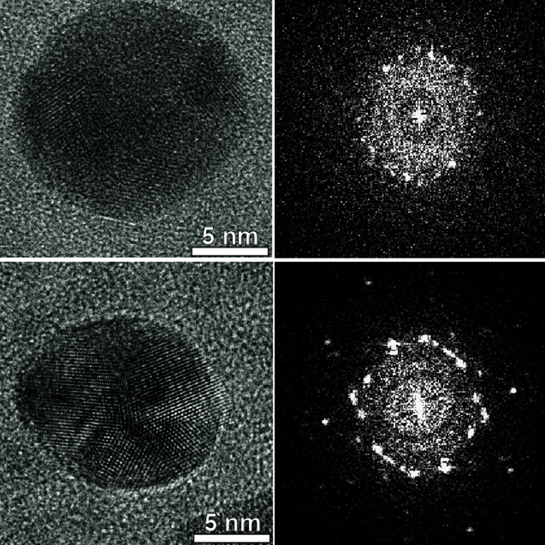
With the new technique, researchers can see resolutions down to around 1.02 angstroms, compared to about 2.36 angstroms in previous experiments. The team said they’ve achieved the highest spatial resolution and spectral visibility recorded in their field to date.
Beyond microscopes, the team hopes to apply their platform technology to other problems, as the technique of encapsulation could apply to any microchip or optical-based technique.
“In any field, thinner is better because you’re getting less information from the thick container compared to the inside object itself,” Koo said.


