Northwestern graduation events set for 2026
October 28, 2025
For the first time, scientists at Northwestern University, Boston University (BU) and University of California, Berkeley (UC Berkeley) have built a tiny photonic quantum system into a traditional electronic chip.
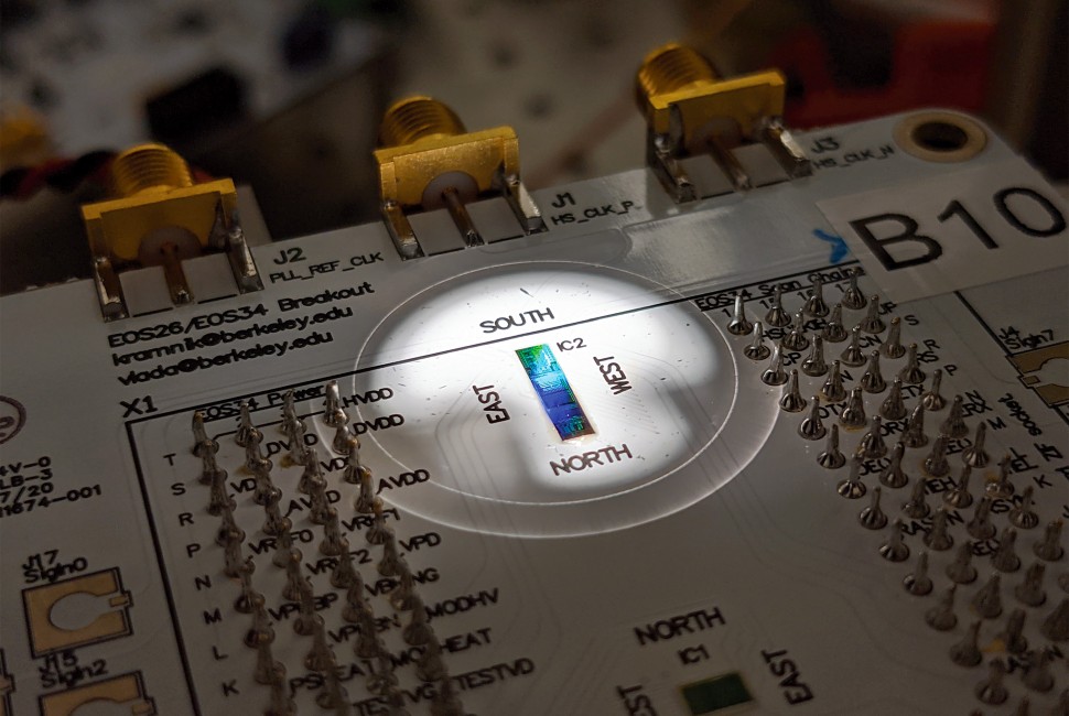
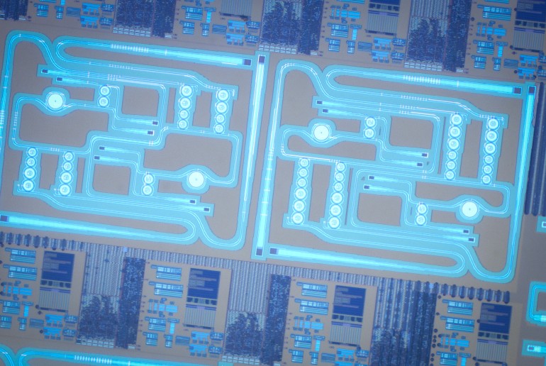
The first-of-its-kind silicon chip combines both the quantum light-generating components (photonics) with classical electronic control circuits — all packed into an area measuring just one millimeter by one millimeter. So, not only does the chip generate quantum light, but it also has its own built-in smart electronic system to keep that light perfectly stable.
This photonic-electronic integration enables the single chip to reliably produce a stream of photon pairs — basic units that encode quantum information — required for light-based quantum communication, sensing and processing.
A commercial semiconductor foundry fabricated the chip, demonstrating its ability to be manufactured for large-scale production.
The study was published in the journal Nature Electronics.
“Quantum experiments in the lab usually need big, bulky equipment, which requires pristine, clean conditions,” said Northwestern’s Anirudh Ramesh, who led the quantum measurements. “We took many of those electronics and shrunk them down onto one chip. So, now we have a chip with built-in electronic control — stabilizing a quantum process in real time. This is a key step toward scalable quantum photonic systems.”
This is a big deal because it’s not easy to mix electronics and photonics.”
“For the first time, we have achieved monolithic electronic, photonic and quantum integration,” said Northwestern’s Prem Kumar, one of the study’s senior authors. “This is a big deal because it’s not easy to mix electronics and photonics. It was a heroic effort that combined expertise from an interdisciplinary, collaborative team of physicists, electrical engineers, computer scientists, materials scientists and manufacturing experts. Our chip could open doors for not only computing but sensing and communication applications.”
An expert in quantum optics, Kumar is a professor of electrical and computer engineering at Northwestern’s McCormick School of Engineering, where he directs the Center for Photonic Communication and Computing. At the time of the research, Ramesh was a Ph.D. candidate in Kumar’s laboratory; now he is a quantum systems validation engineer at U.S.-based quantum computing company PsiQuantum.
Ramesh co-led the study with Danielius Kramnik at UC Berkeley and Imbert Wang at BU. Kramnik, who led the circuit design and electronic integration, is a recent Ph.D. graduate from the laboratory of Vladimir Stojanovíc, an adjunct professor of electrical engineering and computer sciences at UC Berkeley. Wang, who led the photonic device design, is a recent Ph.D. graduate from the laboratory of Miloš Popović, an associate professor of electrical and computer engineering at BU.
With their ability to be manufactured using the same high-volume processes that create billions of transistors for everyday electronics, silicon chips are an ideal platform for light-based quantum systems. But stably operating these tiny quantum optical devices requires capabilities that are not currently standard in a commercial foundry. Slight temperature changes, imperceptible manufacturing imperfections and even heat generated by their own components can completely ruin an entire quantum system. To control these tiny variations, researchers have relied on large, external equipment to stabilize quantum optical devices — making it seemingly impossible to miniaturize full systems.
The generation of quantum light in silicon — which the team used in their foundry-manufactured devices — was first demonstrated in a decades-old experiment from Kumar’s lab at Northwestern. In a 2006 study published in the journal Optics Express, Kumar and his collaborators demonstrated, for the first time, that shining a concentrated beam of light into tiny, appropriately designed channels etched in silicon naturally generates photon pairs. These photon pairs are inherently linked, so they can serve as qubits.
In the new study, the team integrated these tiny, ring-shaped channels — each much smaller than the thickness of a human hair — into the silicon chip. When a strong laser shines into these circular channels, called microring resonators, it generates photon pairs. To control the light, the team added photocurrent sensors, which act like tiny monitors. If the light source drifts due to temperature fluctuations or other disturbances, the sensors send a signal to a tiny heater, which adjusts the photon source back to its optimal state.
Because the chip uses built-in feedback to stabilize itself, it behaves predictably despite temperature changes and fabrication variations — an essential requirement for scaling up quantum systems. It also bypasses the need for large external equipment.
“Our goal was to show that complex quantum photonic systems can be built and stabilized entirely within a CMOS (complementary metal-oxide-semiconductor) chip,” Kramnik said. “That required tight coordination across domains that don’t usually talk to each other.”
To ensure their complex quantum chip could be manufactured using a standard CMOS process, the scientists adopted a clever design strategy. They built the photonic components directly into the existing structures commercial CMOS factories already use to manufacture computer chips.
“We pushed the photonics to work within the strict constraints of a commercial CMOS platform, Wang said. “That’s what made it possible to co-design the electronics and quantum optics as a unified system.”
As quantum photonic systems grow in scale and complexity, these integrated quantum chips could become the building blocks for technologies ranging from secure communication networks to advanced sensing and, eventually, quantum computing infrastructure.
“Quantum computing, communication and sensing are on a decades-long path from concept to reality,” said Popović, a senior author on the study. “This is a small step on that path — but an important one, because it shows we can build repeatable, controllable quantum systems in commercial semiconductor foundries.”
The study was supported by the National Science Foundation, the Packard Fellowship for Science and Engineering and the Catalyst Foundation. Chip fabrication support was provided by Ayar Labs and GlobalFoundries.